
AR and MR devices as the next computing platform

The current state of manufacturing technology

Augmented Reality (AR), Mixed Reality (MR), and Extended Reality (XR) have been on everyone’s lips for some time. The first devices that came onto the market with AR or MR functions were mainly used in the industrial segment. Applications here were in online training, e-learning, and VR-supported maintenance ‒ but sales are still low due to the devices’ bulky shape, heavyweight, and limited Field Of View (FOV). However, the next generation of devices is on the way. Those shall allow interaction between people and the digital universe – eyeglass-like with an integrated mini-computer. The strategic goal: AR and MR devices as the next computing platform. The expectations for the devices are high. Analysts compare the upcoming changes with those of the introduction of the first iPhone in 2007.
There is no question that it is not just technology companies and specialty glass manufacturers dealing with the issue. Leading eye optics experts are investing in researching and developing new intelligent glass products that mix AR with ophthalmic functionalities. Integrating Virtual Reality (VR) and metaverse technologies sets a clear signal for the future: It is possible to interact with the environment via AR, such as quickly and easily accessing certain information, understanding another language, or being guided from A to B by a virtual navigation system.
The simultaneous correction of ametropia opens up further exciting possibilities for many people to improve or recover the ability to see.
However, before the successful market launch of AR devices, there are still a few hurdles to overcome. These arise from the technical challenges of AR/MR, the current state of manufacturing technology, and the increasing importance of the economic aspects.
Since AR and MR devices shall be produced in billions of units, the supply chain will be driven by cost efficiency. The threshold for market acceptance can only be overcome if the end product’s price is affordable and attractive to the consumers. To achieve this, stable and cost-effective manufacturing processes with a high level of automation are required to guarantee a long service life and high reliability of the components.
The display – the core of each AR device
Among the most significant technological challenges associated with AR is the optical design of the device. To allow users to see the natural world and the virtual image in parallel, displays are integrated into the eyeglasses. The so-called optical combiner, which combines the real-world image with the virtual image generated by the display or projector, is at the heart of any AR device.
Already well-known to the industry for decades, such combiners have not been suitable for consumer all-day use, especially their form.
Waveguide technology offers a potential solution: Flat substrates, made of optical grade glass, guide the image parallel to the waveguide’s surface while simultaneously allowing light to pass through perpendicular to the waveguide’s surface.
Thus, many performance-defining parameters depend on the waveguide material and its specifications, such as refractive index, specific density, transmittance, homogeneity, flatness, warpage, etc.
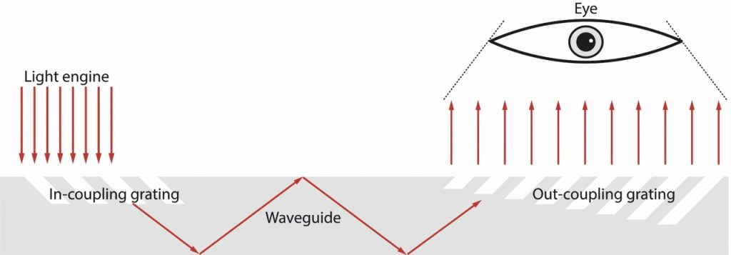
To fabricate lightweight near-eye displays, AR devices use optical waveguides with diffraction gratings to guide light from a display by Total Internal Reflection (TIR) into the human eye’s view.
Figure 1 shows a scheme of the optical gratings used as light couplers. The small input grating diffracts the light coming from a light engine (or projector) into the eyeglass, acting as a waveguide.
The light is diffracted in the viewer’s direction at the out-coupler grating. For uniform illumination of those out-coupling gratings, the structure depth increases with the traveled light distance in the waveguide, also named “leaky gratings.”
Different approaches exist for the design of coupling gratings. One type is the so-called Surface Relief Grating (SRG). Within this group, the gratings are classified into blazed gratings, binary gratings, analog gratings, and slanted surface relief gratings. Slanted gratings suppress higher diffraction orders and thus maximize the light yield. Variation of the slant angle is desirable to achieve a high FOV, but a certain challenge. In the following, the fabrication process of slanted SRGs will be shown.
Manufacturing of slanted surface relief gratings as a crucial component of the waveguide
Ion beam etching technologies are ideally suited for precise surface processing. All ion beam techniques are applied in a vacuum environment. The ion beam process combines physical and chemical etching.
Physical etching uses the kinetic energy of fast inert ions bombarding the surface to sputter, releasing atoms from the target surface. That process is working on all materials facing the ion beam. Chemical etching utilizes a chemical reaction between the reactive ions and the target surface. The reaction products must, therefore, be volatile.
The ion beam scans over the device surface. By varying the scan velocity, thus the dwell time, and the angle of incidence, the material removal can be adjusted precisely at each substrate location to achieve a perfect etching structure with superior homogeneity. It is possible to create many different geometries in a large spectrum of processable materials, including glass, SiO2, SiC, TiO2, etc.
Furthermore, ion beam processing is a contactless process that does not create any mechanical stress on the surface of the substrate, thus avoiding sub-surface damage. That makes ion beam processing the method of choice for low damage, high precision, and high uniformity for optical engineering.

Different ion beam technologies are used to produce slanted surface gratings depending on whether a constant or varying angle is required.
Reactive ion beam etching for processing SRGs with a constant slant angle and etching depth
In the first step, a resin mask or pattern on a glass substrate is created by photolithography. The mask will be used to structure an intermediate metal mask or the glass directly.
A full substrate processing by Reactive Ion Beam Etching (RIBE) is ideally suited to create surface relief gratings with constant slant angles.
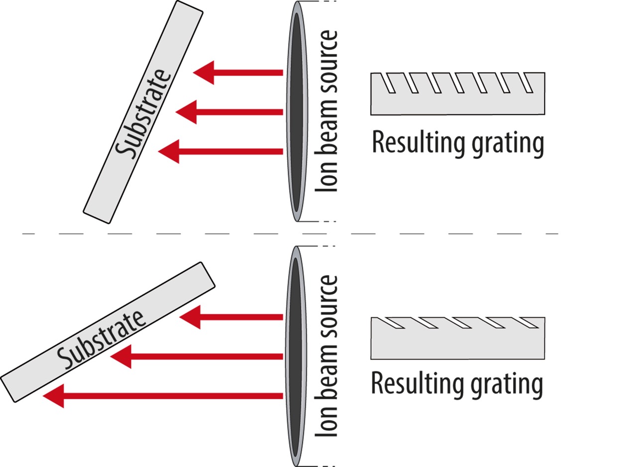
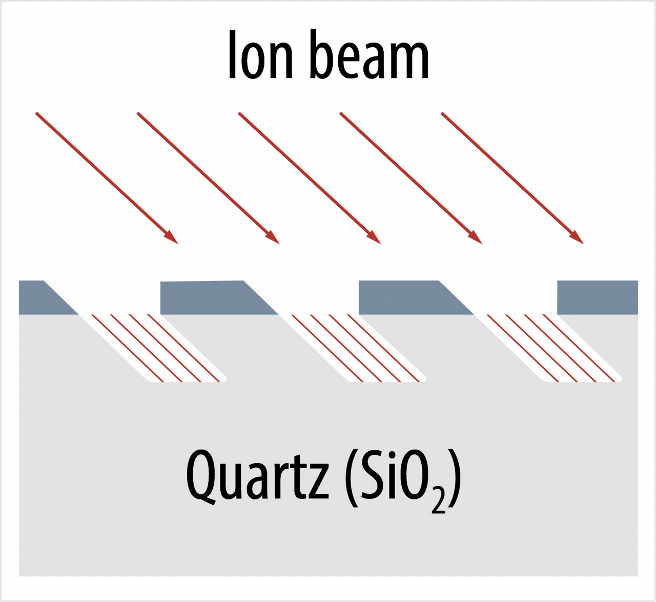
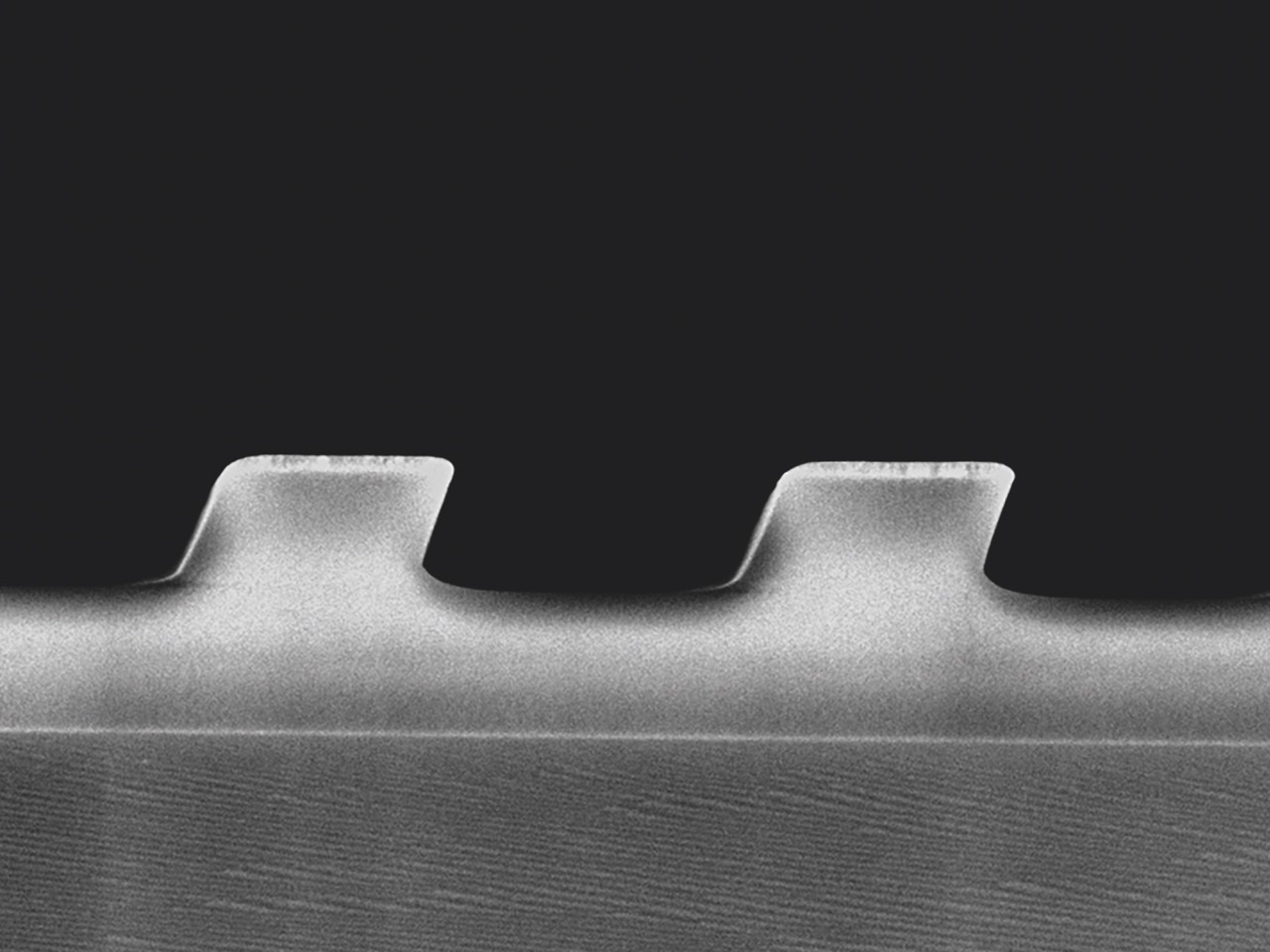
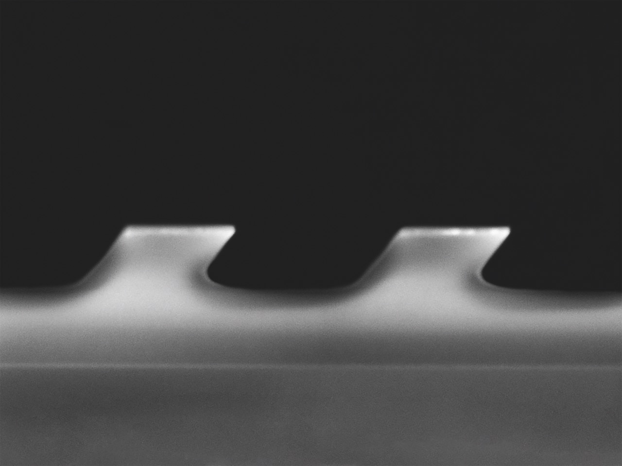
Introducing reactive gases into the etching process makes it possible to control the selectivity of different surface materials and enhances the etch rate. The substrate can be tilted to etch slant angles as flat as 60 degrees (Fig. 2). On top of the substrate material is a chromium mask, which defines the grating structures (Fig. 3).
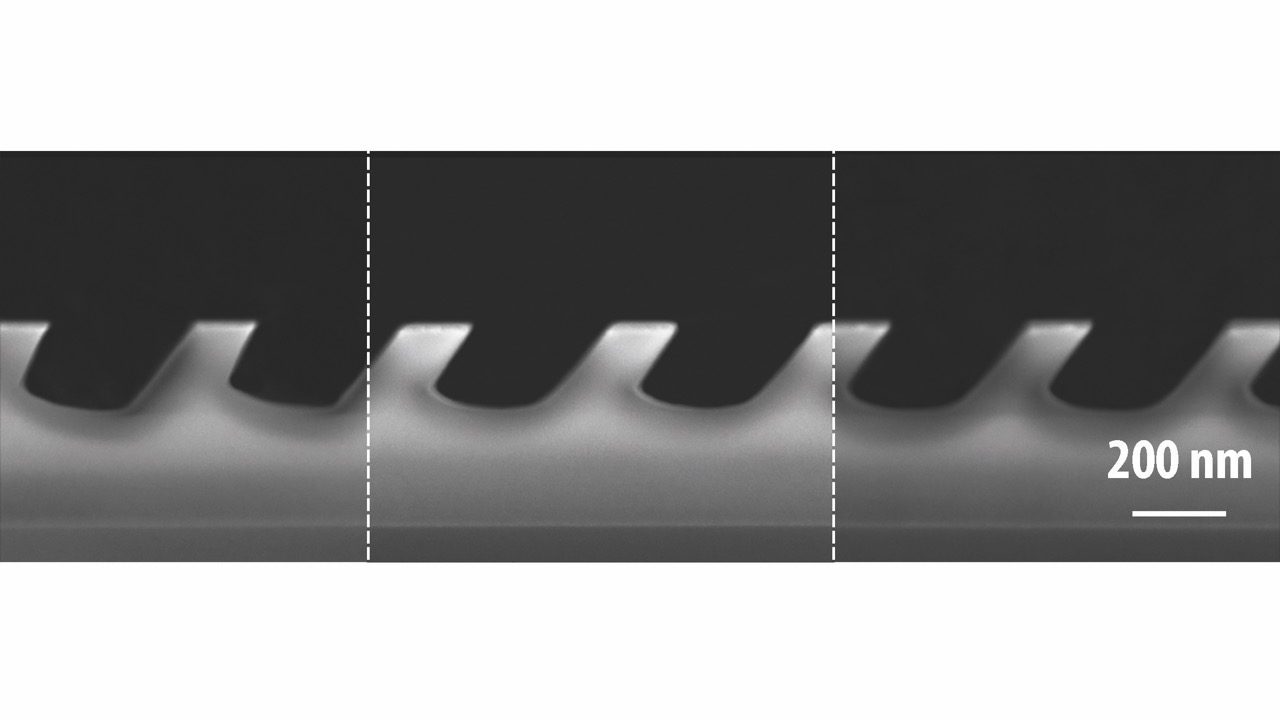
Crucial parameters for the RIBE process are the selectivity between mask and substrate and the geometry control of both the side wall and bottom angles. Using different etching gases can control the degree of anisotropic etching behavior, which finally defines the resulting geometry of the gratings (Fig. 4). Reactive gases can be introduced into the ion beam source. The ability to independently control ion energy and ion current is additionally used to adjust slant geometry and selectivity.
Another advantage of the RIBE process for manufacturing surface relief gratings is that a wide FOV is needed for the final AR product. The critical angle for total internal reflection limits the shallowest angle under which light may travel within the waveguide. The critical angle is smaller for high refractive index materials, and the FOV is bigger. That is why high-refractive materials with refractive indices >2 will not be etched with standard gases like those used for quartz etching but with adapted mixtures and recipes.
These unique capabilities to control gas mixture, ion energy and ion current, substrate angle, and even substrate temperature make RIBE the preferred technology for etching slanted relief gratings.
Reactive Ion Beam Trimming (RIBT) for processing SRGs with varying slant angle and etching depth
Variation of the slant angle is desirable yet somewhat challenging to achieve a high FOV. Ion Beam Trimming (IBT), a well-established technique in the semiconductor industry to locally modify a given substrate’s thickness to achieve a desired target topography, is ideally suited to create surface relief gratings with varying slant angles and etch depths. IBT uses a focused broad beam of positively charged ions to etch material locally off the glass substrate by ion bombardment.
An ideal-shaped ion beam ensures a sufficient lateral resolution and a high throughput. The ion beam moves in a meander-shaped pattern across the substrate surface during trimming. It is possible to adjust the material removal precisely by altering the local dwell time.
Reactive Ion Beam Trimming (RIBT) has been adapted to fabricate surface relief gratings with varying slant angle and trench depth. The optically transparent substrate is covered with a hard mask providing the basic grating geometry such as period and duty cycle. Then, localized ion beam etching is applied to etch the trenches.
Varying the ion irradiation dose using dwell time variations sets the trench depth locally. The angle of incidence of the ion beam directly transfers into the substrate as the slant angle. It can be varied independently of the dwell time, providing the unique possibility of achieving a continuous variation of the slant angle across one die.
To avoid redeposition of the sputtered trench material to the grating side walls, additional reactive gases are added to the ion beam source. The plasma activation of the reactive gases leads to a chemical and physical etching of the substrate material, which helps to increase throughput, material selectivity, and trench angles of patterned surfaces.
The choice of the process parameters, e.g. process gas composition and ion energy, allows for tuning the selectivity between the hard mask and optical material such that high aspect ratio trenches are possible while keeping the hard mask thin. That avoids the shadowing of neighboring structural features.
Direct structuring of waveguides vs. structuring of master stamps
The slanted gratings can either be etched directly into the waveguide or into a master stamp (mold) that is used to produce the AR/MR display via nanoimprint lithography (NIL). For NIL, a master stamp is structured by RIBE technology. Afterwards, the master stamp is pressed into a polymer spin-coated substrate to replicate the pattern.
However, polymers do not offer high-refractive indices as glass material can do, which has a disadvantage regarding the FOV of the final device.
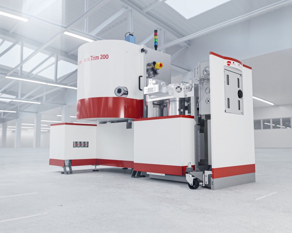
scia Systems offers industrial-approved solutions to meet customers’ demand for high-quality waveguide or master stamp patterning.
The systems are used for coating, etching, and cleaning processes with nanometer resolution and have been successfully implemented in various high-tech industries worldwide, including microelectronics, MEMS, and precision optics industries. ◆

Mandy Gebhardt
Mandy Gebhardt holds a diploma degree in Economic Computer Science from the University of Cooperative Education Glauchau. Since 2000, she worked in marketing and public relations in various high-tech companies, and since 2010, as Team Leader of Marketing/PR. In October 2023, Mandy joined scia Systems as the Head of Marketing.
scia Systems offers industrial-approved solutions for high-quality waveguide or master stamp patterning. The systems are used for coating, etching, and cleaning processes with nanometer resolution and have been successfully implemented in various high-tech industries worldwide.

Matthias Nestler
Matthias Nestler holds a diploma degree in Physical Engineering from the West-Saxonian University of Applied Sciences Zwickau. After graduating in 2000, he worked as a project manager in a company specializing in ion beam and plasma process technologies. In 2004, Matthias took the product manager position in this technology field. After founding in 2013, he joined scia Systems as Director of Products and Technologies. Since then, he has been responsible for all product and process development activities.